From Breadboard to PCB: Turning Your Prototype into Reality
Every great invention starts with an idea—and in electronics, that idea often takes its first shape on a breadboard. Breadboards are the ultimate playground for experimentation, allowing you to test and tweak your circuit until it works just the way you want. But once you’ve nailed down your design, it’s time to move from the temporary, sometimes messy breadboard setup to a sleek and durable printed circuit board (PCB).
Transitioning from breadboard to PCB can seem daunting at first, but with the right tools and guidance, it’s a rewarding journey that transforms your prototype into a professional-looking, reliable product. Whether you’re working on a personal project or preparing for a commercial launch, this guide will walk you through the process step by step.
Why Move from Breadboard to PCB?
Breadboards are great for prototyping, but they come with limitations:
- Fragility: Loose wires and connections can cause inconsistent performance.
- Size: Breadboards aren’t ideal for compact designs or portable devices.
- Durability: Breadboards aren’t built to last, especially for projects with frequent use.
A PCB addresses these issues, providing a stable, compact, and professional-looking solution that’s perfect for long-term use.
I still remember the first time I turned a breadboard project into a PCB. It was a simple temperature sensor, but seeing it on a neat little board instead of a tangle of wires felt like a major accomplishment.
Step 1: Finalize Your Breadboard Design
Before diving into PCB design, make sure your breadboard circuit is 100% functional. Test it thoroughly to identify any bugs or areas for improvement.
Checklist for Finalizing Your Prototype:
- Does the circuit perform reliably under different conditions?
- Are the components properly rated for voltage and current?
- Have you minimized unnecessary components to keep the design simple?
Once you’re satisfied with your design, document everything. Take pictures, draw a schematic, and note any special considerations. Trust me, having detailed records will save you from headaches later.
Step 2: Create a Schematic Diagram
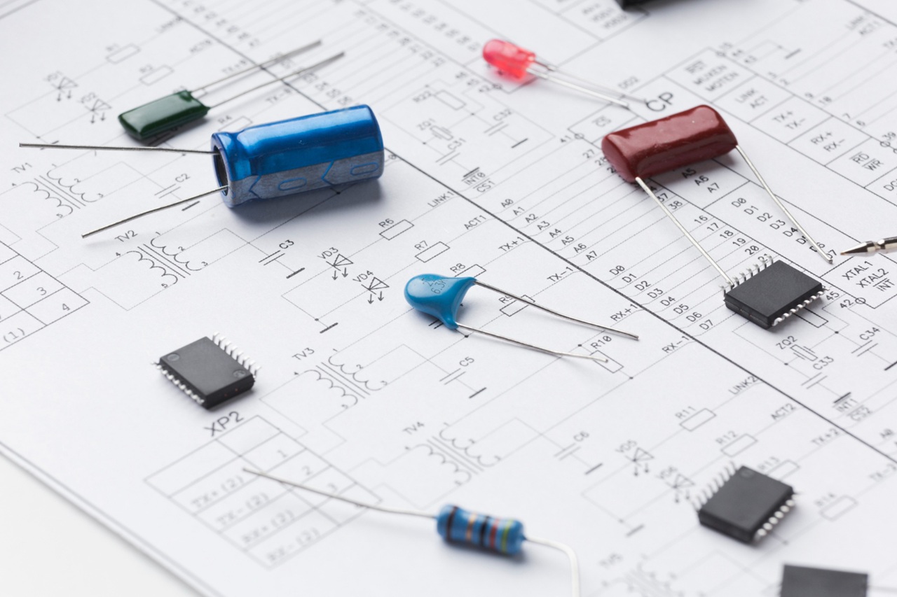
A schematic diagram is a blueprint of your circuit. It shows how components are connected without worrying about physical layout.
Tools for Schematic Design:
- KiCad: Free and open-source, great for beginners and professionals.
- Eagle: Offers powerful features with a beginner-friendly interface.
- Fritzing: Ideal for transitioning from breadboards, with a focus on simplicity.
When designing your schematic, label everything clearly. This includes component values (e.g., resistors: 220Ω, capacitors: 10μF) and connections. Think of the schematic as your project’s DNA—it’s what you’ll use to guide the PCB layout.
Pro Tip: Double-check your schematic against your breadboard circuit. It’s easy to miss a connection or component when translating to a digital format.
Step 3: Design the PCB Layout
Now comes the fun part: designing the physical layout of your PCB. This is where your schematic gets transformed into a real-world board.
Steps for PCB Layout Design:
- Import Your Schematic: Most software allows you to import your schematic directly into the layout tool.
- Place Components: Drag and drop components onto the board, positioning them logically and compactly.
- Route Traces: Connect the components with copper traces, replacing the wires used on the breadboard.
- Add Labels and Mounting Holes: Include labels for pins or connectors and holes for mounting your PCB in an enclosure.
Tips for a Good Layout:
- Keep high-current traces wider to handle the load.
- Separate analog and digital sections to reduce interference.
- Avoid overlapping traces to prevent short circuits.
When designing my first PCB, I learned the hard way that poor trace routing can lead to a messy, error-prone design. Spending extra time on neat routing made all the difference.
Step 4: Validate Your Design
Before sending your PCB for manufacturing, validate the design to catch potential errors.
Common Tools for Validation:
- DRC (Design Rule Check): Built into most PCB design software, this checks for issues like overlapping traces or incorrect spacing.
- Simulations: Some tools let you simulate the circuit to ensure it behaves as expected.
Personal Anecdote: On my first PCB, I forgot to connect the ground plane to all components. The result? A non-functional board that taught me the importance of triple-checking every connection.
Step 5: Manufacture Your PCB
Once your design is ready, it’s time to bring it to life. Many PCB manufacturers offer affordable services, even for small orders.
Popular PCB Manufacturers in 2025:
- JLCPCB: Affordable with quick turnaround times.
- PCBWay: Excellent for custom designs and small batches.
- OSH Park: Ideal for hobbyists with small, simple boards.
Most manufacturers will require you to upload Gerber files, which are the standard format for PCB designs. Your design software can export these files.
Pro Tip: Use online previews to check your Gerber files before submission. Some manufacturers offer built-in viewers to ensure everything looks correct.
Step 6: Assemble Your PCB
When your PCBs arrive, it’s assembly time! Depending on your design, this could involve soldering through-hole components, surface-mount devices (SMD), or a mix of both.
Soldering Tips:
- Use a fine-tipped soldering iron for precision.
- Apply just enough solder to secure the connection without creating bridges.
- Test each soldered component with a multimeter before moving on.
I still find assembly to be one of the most satisfying parts of the process. There’s something therapeutic about watching your PCB come to life piece by piece.
Step 7: Test the Final Product
Before declaring victory, test your assembled PCB to ensure it works as intended.
Testing Checklist:
- Check for shorts or open circuits using a multimeter.
- Power up the board and test functionality.
- Use oscilloscopes or logic analyzers for advanced troubleshooting if needed.
If something doesn’t work, don’t panic. Debugging is a normal part of the process. Revisit your schematic, PCB layout, and assembly to pinpoint the issue.
Anecdote: My first PCB had a reversed LED. It took an hour of head-scratching and a multimeter to figure out the problem, but fixing it was incredibly satisfying.
Step 8: Package and Protect
For a polished finish, consider adding an enclosure to protect your PCB and enhance its appearance. Enclosures can be 3D-printed, purchased online, or repurposed from everyday items.
Pro Tip: If you plan to mass-produce your project, design custom enclosures that align with your PCB dimensions.
Final Thoughts
Turning a breadboard prototype into a PCB is a transformative experience. It’s a journey that sharpens your skills, deepens your understanding of electronics, and results in a tangible, professional-looking product.
Whether you’re creating a one-off gadget for yourself or planning to share your creation with the world, the transition from breadboard to PCB is a major milestone worth celebrating.
So, pick a project, follow these steps, and watch your idea come to life—one trace at a time.
Happy building!


Post Comment